Magnum Technologies Pty Ltd.

PCB Fabrication

PRINTED CIRCUIT BOARD (PCB)

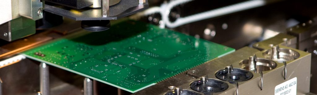
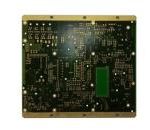
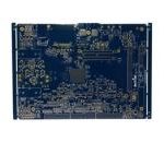
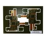
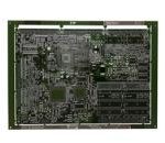
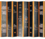
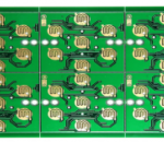
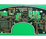
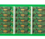
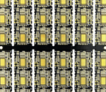
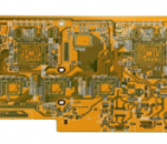
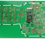
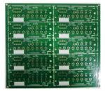
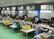
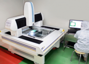
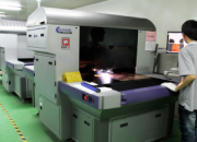
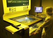
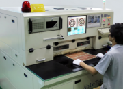
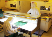
Magnum enjoys over 15 years of reputation as a PCB supplier of high quality standards and competitive pricing. We are qualified and experienced to use standard FR-4, high Tg, halogen free and high speed/ultra low loss materials. Our clientèle extends to medical, gaming, telecommunication and industrial electronics.

Range of PCBs

  • Double sided PCBs
  • Multilayer up to 16 layers
  • RoHS compliant (Tg>170°C) PCBs
  • High Density Interconnect PCBs
  • Flexible
  • Rigid-flex PCBs

Specialization

  • Advanced high layer line card
    • High performance standard/mid/low loss and Green materials
    • Advanced registration system for tight D2M design 
  • Sequential build up
    • N+N, N+M+N structure
    • Sequential line card technology for high speed application
  • High layer backplane
    • Backplane board size up to 40″x20″
    • Provider for Telecom
  • HDI line card
    • Large format System HDI board

Value Added Services through Product Life Cycle

  • R&D
    • Design for manufacturing
    • Material selection
    • Panelization
    • Optimization 
  • New Product Introduction (NPI)
    • Prototyping
    • Pilot testing
    • Technical support on issues emerging from prototyping
  • Production
    • Cost-effective solution
    • Reduced lead time
    • Price reduction
  • Maturity
    • High volume
    • Improve yield and further cost reduction

PCB Product Overview

Materials

Type of Lamination

Model

Type of Lamination

Model

Normal Tg

SYL S1141

MICA EG 150T

PANASONIC R1755C

High Tg w/ Filler

SYL S1000-2

MICA HR-02

PANASONIC R1755V

NELCO N4000-29

Middle Tg

SYL S1141KF

SYL S1000

MICA LA-02

Mid/Low Loss

ISOLA FR408, FR408HR

NELCO N4000-13, 13SI, 13 EP

MITSUBISHI EL-190T

HITACHI MCL-HE-679G

Halogen Free

SYL S1155

R-1566W, WN, V

NPGN 150, 170

Ultra Low Loss

ROGER 4350/4000

PANASONIC MEGTRON 6

High Tg

SYL S1170

MICA HR-01

PANASONIC R1755V

PTFE

TACONIC RF-35A2

Production Capabilities

Elements

Capability

Elements

Capability

Max. circuitry width

564mm

Base copper weight (Inner layer)

1/3oz – 4oz

Max. circuitry length

1021mm

Base copper weight (Outer layer)

1/4oz – 3oz

Max. layer count

20

Press-fit hole size tolerance

± 0.05mm

Max. board thickness

8mm

Aspect ratio (Line card)

15:1

Max. board thickness tolerance

± 8%

Aspect ratio (Back panel)

16:1

Routing outline tolerance

± 10mm

Type of Finishes

Impedance ≤ 50Ω
Impedance ≥ 50Ω

+/- 8%
+/- 4Ω

Single Surface Finishes

ENIG (Autotech CNN/ NPR-8)

Electrolytic Nickel Gold Plating

Immersion Tin (Stanntech)

Immersion Silver (Sterling)

OSP (Entek Plus HT), HASL

Min. inner trace spacing (Line card)
Min. inner trace spacing (Back plane)
Min. outer trace spacing (Line card)
Min. outer trace spacing (Back plane)

0.075/0.075mm
0.075/0.075mm
0.075/0.090mm
0.100/0.114mm

Dual Surface Finishes

ENIG (Autotech CNN) + OSP

Tab gold (G/F) + I-Silver

Tab gold (G/F) + HASL

Tab gold (G/F) + OSP

Production Lead Time

Lead Time (Days)
Layer Standard Protos Express Protos Mass Production
2 5 3 10
4 6 3 14-21
6 7 4 18-21
8 8 5 21-24
10 10 6 23-26
12 and above 12 6 From 30

*The above lead times excludes transit time to destination

Reliability Testing & Analysis

Testing Equipment:

  • SIR tester
  • Hi Pot tester
  • Wet force balance
  • Temp cycling chamber
  • SPP testing
  • Akrometrix 3D flatness tester
  • ATC chamber
  • LCR tester
  • HAST
  • Thermograph
  • RoHS tester
  • IST tester
  • TMA tester
  • Ionic contamination chamber

Analysis Equipment:

  • IR reflow
  • Wave soldering
  • SEM & EDX

Industries Served

Industries Served

We serve the following industrial sectors:

  • Medical
  • Telecommunication
  • Gaming
  • Industrial electronics

Certification